The Challenges of Wearable Electronics Circuit Diagram
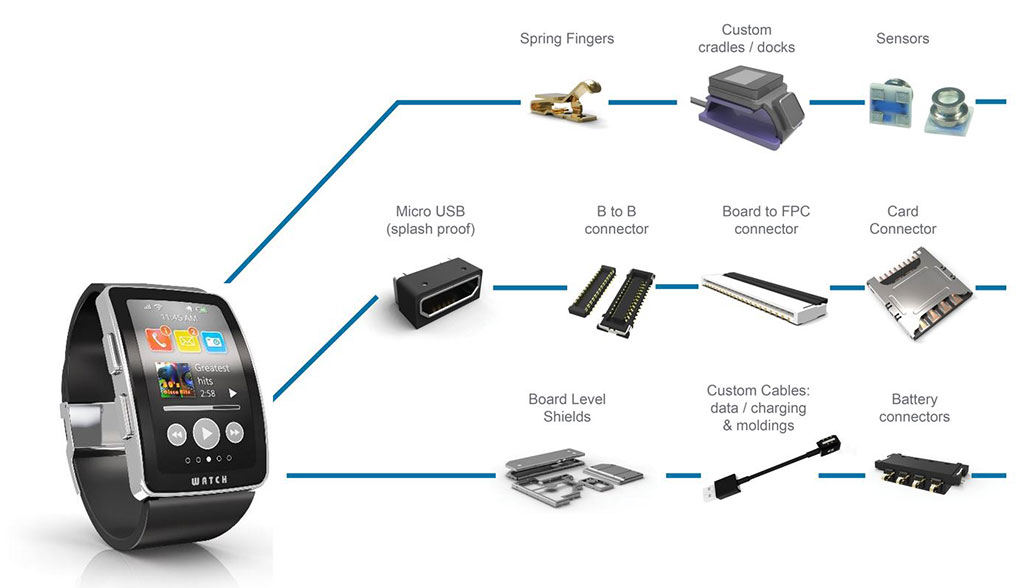
The Challenges of Wearable Electronics Circuit Diagram Developing a wearable electronic product involves juggling design constraints and compromises in ways that are quite different from more conventional designs. This article discusses the main design tradeoffs for wearable technology products. Putting all the components together will commonly require multiple thin-substrate PCB's that are Solutions from Molex include Quad-Row Connectors that save up to 30% of PCB space, IP67/68/69-rated interconnects for durability and advanced designs to prevent damage during assembly and use. Flexible floating connectors and compact layouts provide design versatility, while robust performance supports seamless integration of advanced features.
Wearable Electronics Our industry experience — combined with our state-of-the-art technology and advanced materials — makes us the perfect choice for your next wearable electronics PCB project. We also have extensive experience with the concept of miniaturization and will work with you from the initial design of a project through to the

Design Notes for Wearable PCB Design Circuit Diagram
Designing a wearable product can be difficult for any design engineer, because the rules for most electronics don't necessarily apply to the world of wearables. PCB companies are acutely aware of the difficulties and hurdles that must be overcome in order to create a proper PCB for the wearable market.
The explosive growth of wearable technology and ubiquitous computing has revolutionized how we interact with electronic devices. This transformation has brought unique challenges and opportunities in printed circuit board (PCB) design and manufacturing. This comprehensive guide explores the essential aspects of designing PCBs for wearables and ubiquitous computing applications, focusing on Printed circuit board (PCB) design is at the center of electronics product development. When creating small gadgets like fitness trackers and other wearable technology devices, it's especially important for design software like Fusion to include detailed PCB capabilities and electronic behavior simulation.
How to Design a Wearable Technology Product Circuit Diagram
Normally, layer count varies from four to eight layers for wearable devices. Layer structuring is such that if it's an eight layer PCB, it provides enough ground and power plane to sandwich the routing layers. Thus, the ripple effect in crosstalk is kept to a minimum and electromagnetic interference or EMI is significantly reduced. Read the Altium Ebook on wearable electronics and PCB Design. Until recently, wearable accessories had one primary purpose-- to be fashionable. Sure, watches are useful for keeping time and staying punctual, but that's about as far as things went for functionality. Today, we have a rising selection of wearable electronics, many of which can be